Turbocharging AlN/GaN HEMTs

Engineers from Ohio State University are claiming to have opened the door to the fabrication of far smaller AlN/GaN HEMTs operating at much higher frequencies.
The team’s breakthrough involves the combination of in-situ passivation and the addition of re-grown heavily doped n-type contacts using a selective etching process.
AlN/GaN HEMTs are a very promising class of transistor for RF and power devices. Compared with the more conventional AlGaN/GaN form of the III-N HEMT, they are free from alloy scattering and have far higher values for electron mobility and the density of the two-dimensional electron gas – up to 4 x 1013 cm-2, and between 1000 cm2 V-1 s-1 and 1800 cm2 V-1 s-1, respectively.
Back in 2010, Keisuke Shinohara and co-workers from HRL Laboratories reported values for the cut-off frequency and maximum oscillation frequency of AlN/GaN HEMTs of 220 GHz and 400 GHz, respectively. According to the engineers from Ohio, an even better performance could come from scaling the source-drain spacing. However, this is not easy with the conventional process, involving re-growth and a lift-off step using SiO2.
The Ohio approach is claimed to offer an alternative that facilitates the production of aggressively scaled HEMTs with a very low contact resistance.
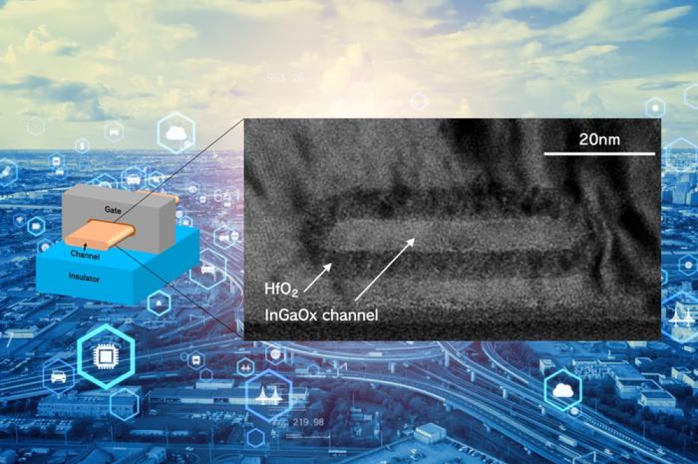
To demonstrate the potential of their novel process, the engineers from Ohio have produced AlN/GaN HEMTs from epiwafers featuring an AlN nucleation layer, a 1.5 mm-thick semi-insulating buffer, a 100 nm-thick unintentionally doped GaN channel, a 5.8 nm-thick barrier and a 4.3 nm-thick in-situ SiN layer. According to Hall effect measurements, the two-dimensional electron gas in this epistructure has a carrier density of 2.2 x 1013 cm-2 and an electron mobility of 1060 cm2 V-1 s-1.
Device fabrication began with selective etching to expose the sidewalls of the two-dimensional electron gas and enable a source-to-drain spacing of 3 mm. After applying gallium polishing to desorb sub-oxides from the surface and the sidewalls of the two-dimensional electron gas, the team loaded the processed epiwafer into an MBE chamber and deposited a layer of heavily doped n-type GaN, grown to a height that leads to an extension above the SiN surface of 20 nm. This approach is designed to ensure sidewall contact with the two-dimensional electron gas. Chemical etching selectively removed the polycrystalline GaN formed on the unetched in-situ SiN layer to expose the active region for the gates.
The team has analysed the quality of its processed wafers by various forms of electron microscopy, and found no obvious dislocations or boundaries at the etched edge and regrowth interface, suggesting high-quality lattice-matched n-type GaN re-growth.
To complete the fabrication of the AlN/GaN HEMTs, the team used plasma-etching to form a mesa, employed electron-beam evaporation to add non-alloyed metal stacks on the regrown GaN regions, and formed 0.7 mm Ni/Au gates by optical lithography and electron-beam evaporation.
Scrutinising these transistors with a focused ion-beam scanning tunnelling electron microscope revealed a straight and clear interface between titanium and SiN. This suggests that processing did not cause any breaking or damage to the thin SiN layer, so it can fulfil its role of preventing the
AlN surface from being exposed.
Scanning electron microscopy images reveal that the edge definition for the regrown n-type GaN is straight and clear with sharp acuity. In contrast, images for a control device produced with a conventional lift-off process uncover irregular and rough edges, a weakness that hampers aggressive device scaling.
Hall effect measurements on the HEMTs produce similar values to those on the epiwafers, indicating that processing did not induce surface damage.
The engineers measured an interface resistance of 0.058 Ω mm, which is close to the theoretical value. Based on this finding, the team suggests that their etching process does not degrade the interface between the regrown n-type GaN and the etched two-dimensional electron gas sidewall.
Electrical measurements on HEMTs with a gate length of 0.7 µm determined a maximum transconductance of 0.25 S mm-1, and a linear fit and extrapolation suggest a threshold voltage of -4.9 V. The maximum drain current is 1.57 mA mm-1, and there’s an on-resistance of 1.85 Ω mm at a gate voltage of 1 V. Breakdown voltage is 23.3 V, similar to that for control devices produced with conventional
process, suggesting that the engineer’s selective etching process does not degrade breakdown performance.
Pictured above: Schematic epitaxial stack of in situ SiN/AlN/GaN HEMTs
Reference
C. Cao et al. Appl. Phys. Express 18 036501 (2025)